Home02 · The HostVenkat's Journey
My journey
From a polytechnic in Sivakasi to the fabs India is about to build.
I did not arrive in semiconductors through a campus placement. I arrived through a diploma, a mill, a seating factory and a one-way ticket to Singapore. Every step since has been learned on a floor, next to a machine, with someone patient enough to show me. This is that route, and the ladder it turned out to be.
Where hands came first
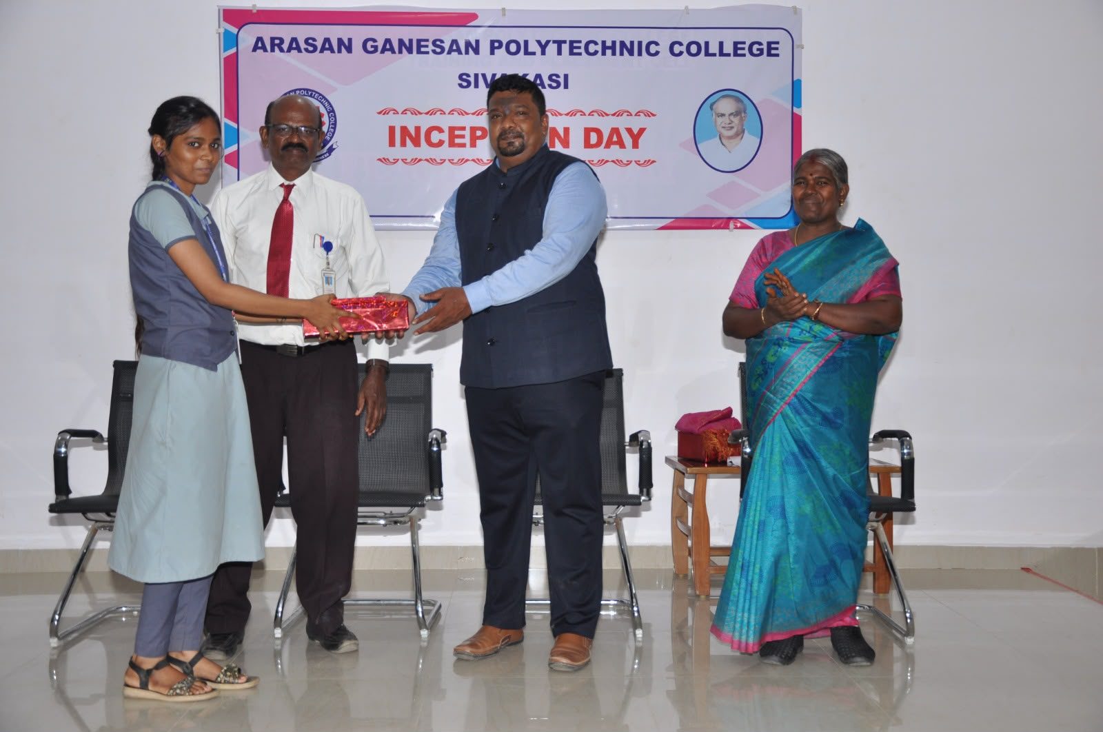
A fireworks and printing town in southern Tamil Nadu. Arasan Ganesan Polytechnic gave me a diploma in electrical and electronics; a spinning mill and a seating-systems plant gave me the habit of fixing what is in front of me.
Where the fab became home
Nine years across Infineon, ASE and Micron: wafer probe, final test, first-silicon bring-up, and finally a 300 mm fab startup where I led a CVD module team through 100+ tool installations.
Where the building begins
Training programmes, 450+ engineer teams for global OEMs, the HCL–Foxconn ATMP/OSAT DPR, and now PTW India, the equipment and infrastructure services company for India's fabs.
The route
Twenty-two years, one apprenticeship.
Each stop carries a "learned by doing" note: the one lesson that only that floor could teach.
OCT 2001 – MAR 2003 India
Electrical Supervisor
Raja Lakshmi Spinners Pvt Ltd
Motors, drives, panels and the discipline of keeping a spinning mill running through the night.
MAR 2003 – MAR 2004 India
PED Technician
Harita Seating Systems
Production engineering on an automotive seating line: fixtures, cycle time, and the first taste of manufacturing discipline.
MAR 2004 – FEB 2008 Singapore
Production Specialist, Final Test & Wafer Probe
Infineon Technologies
Set up, ran and troubleshot Teradyne (J750, J971/J973, Catalyst) and Advantest test systems, probers and handlers. Part of 100+ new ATE installations for a new facility. Worked with the silicon design team on first-silicon bring-up of 16/32-bit microcontrollers, probe cards and DIB boards, characterisation, reliability and release to manufacturing. Trained new hires as their OJT buddy.
MAR 2008 – APR 2010 Singapore
Senior Engineering Technician, Final Test & Wafer Probe
Advanced Semiconductor Engineering (ASE)
Managed 90+ production specialists and 30+ setup technicians across wafer- and IC-level test equipment. Sustained product on line with SPC/FDC monitoring and guided process engineers through new-equipment qualification.
JUL 2010 – JUN 2013 Singapore
CVD PEE Technologist, Shift Lead (300 mm, 40/22 nm)
Micron Semiconductor Asia
Led the Fab CVD module engineering team through the Fab10 startup: 100+ new equipment installations, facility hookups and qualification, released for production. Managed a 200+ member team across CVD and metrology in a fully automated 12-inch fab. AMAT Producer GT/SE, Lam Express, Extreme, Altus Max and more, TEL SOD; HARP, BPSG, AC/TC and SOD processes. PECVD SAT/LAT and warranty support across Asia and Europe with Applied Materials at >95% uptime. Earlier, 200 mm to 300 mm fab conversions at Tech Semiconductor with AMAT, TEL, Novellus and Lam.
JAN 2014 – MAR 2016 India
Engineering Project Leader, Training & Development
Opus Mind Technologies
Came home to turn nine years of fab experience into curriculum: hands-on semiconductor training programmes for engineers entering equipment and manufacturing roles.
2016 – 2017 India
Semiconductor Equipment Engineer, then Senior Engineer
Orbit Technology Solutions
Managed a 120+ member team of SMEs, product-support and customer-support engineers, lab technicians and design engineers for multiple semiconductor OEM customers. End-to-end installation and engineering operations for CVD, PVD, Etch, CMP, ALD and metrology equipment; PM, CM and troubleshooting to sustain fab process tools.
OCT 2017 – JAN 2023 India · Global
Technical Project Manager, Semiconductor
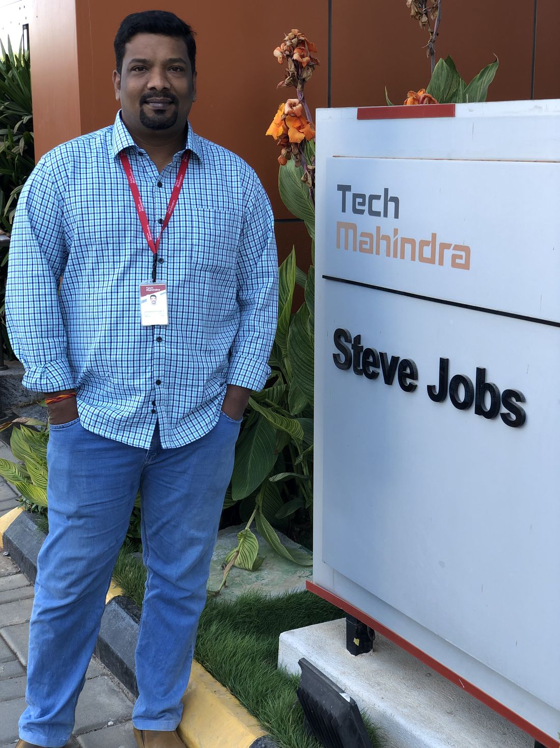
Tech Mahindra · clients AMAT, Lam, ASML, TEL, KLA, Intel, Micron, SCL
Built and managed teams of up to 450+ engineers and specialists supporting semiconductor OEM and fab operations across business units. Directed cleanroom setup, facility integration and metrology tool installations. Ran installation, commissioning, FAT qualification and warranty programmes in India and global fabs with >95% uptime, and global deployment programmes across the US, China, Korea, Taiwan, Singapore, Japan and India. Prepared RFPs, DPRs and business proposals for new semiconductor engagements.
JAN 2023 – APR 2025 India
Group Technical Manager, Semiconductor Manufacturing Practices
HCL Technologies (Sankalp Semiconductor)
Led the Detailed Project Report, planning, stakeholder coordination and government approvals for the proposed HCL–Foxconn ATMP/OSAT facility. Directed facility design, build and operational-readiness programmes: ATMP/OSAT, R&D and ATE labs, equipment build centres, EPCM, MEP, cleanroom readiness and commissioning. Established six offshore development centres and built a 500+ member equipment and process engineering workforce. Directed AI-enabled manufacturing capability development.
JUN 2025 – PRESENT Bengaluru
General Manager, India
PTW Asia Pvt Ltd
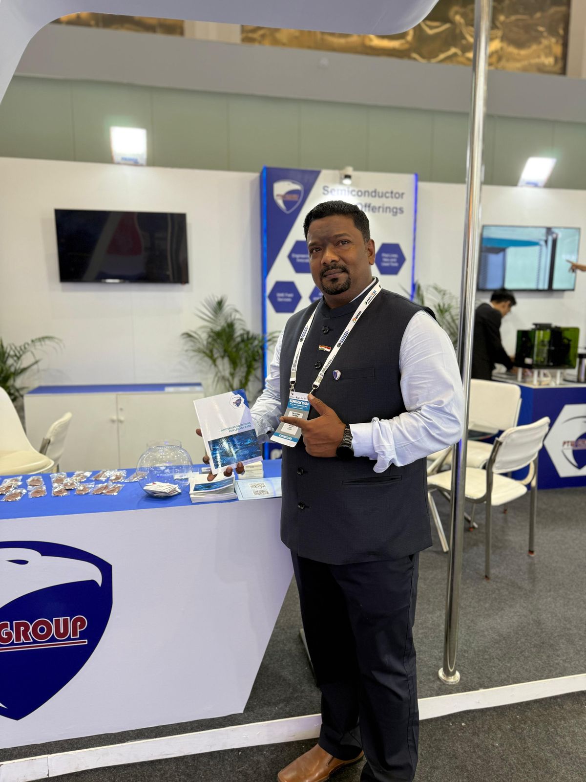
Established and lead PTW India: semiconductor equipment engineering and lifecycle services, installation to decommissioning, fab automation and operational support. Trusted advisor on facility planning, cleanroom readiness, tool-install strategy and Owner's Engineer, PMC and PMCM services including technical due diligence. Acquired and support 10+ customers across semiconductor, solar and lab-grown diamond manufacturing while supporting PTW's global operations.
Interactive module 04
The Learning Ladder
Seven rungs from technician to ecosystem builder. Click a rung to see what it teaches you by doing, what it unlocks, and where I stood on it.
RUNG 01 · TECHNICIAN · 2001 – 2004
You learn that the machine is the teacher.
Electrical supervisor in a spinning mill, then a production engineering technician. No simulator, no sandbox: a motor that trips at midnight and a line supervisor waiting.
RUNG 02 · PRODUCTION SPECIALIST · 2004 – 2008
You learn what "qualified" means.
Testers, probers and handlers on a wafer-test floor. Setups, conversions, correlation lots, and the first time a new tool is released to production with your name on the checklist.
RUNG 03 · SENIOR TECHNICIAN · 2008 – 2010
You learn to run a floor, not a tool.
Ninety production specialists, thirty setup technicians, three shifts. The tool is no longer the unit of work; the shift is.
RUNG 04 · TECHNOLOGIST & SHIFT LEAD · 2010 – 2013
You learn to start a fab.
A 300 mm fab at 40/22 nm, and a module to bring up from an empty ballroom: install, hook up, qualify and release 100+ tools, then keep them above 95% uptime.
RUNG 05 · EQUIPMENT ENGINEER & PROJECT LEADER · 2014 – 2017
You learn to teach, then to run a service team.
Back in India: curriculum first, then a 120+ member engineering team serving multiple OEM customers across CVD, PVD, Etch, CMP, ALD and metrology.
RUNG 06 · PROGRAM & PRACTICE LEAD · 2017 – 2025
You learn that the document is the facility.
Teams of 450+ and 500+ across seven countries. RFPs, DPRs and government approvals. Cleanroom setup, EPCM, MEP and commissioning across multiple infrastructure projects, including the HCL–Foxconn ATMP/OSAT DPR.
RUNG 07 · GENERAL MANAGER & ECOSYSTEM BUILDER · 2025 –
You learn to build the organisation that builds fabs.
PTW India from zero: engineering delivery, EHS, commercial execution, partnerships and 10+ customers in the first year, plus the ecosystem work with government, academia and industry bodies.
Education & credentials
Still a student. Deliberately.
I am completing a Bachelor of Electrical & Electronics Engineering at Anna University while running a company. Experiential learning is not a substitute for fundamentals; it is what makes them stick.
- Bachelor of Electrical & Electronics Engineering (pursuing), Anna University, India
- Diploma in Electrical & Electronics Engineering, Arasan Ganesan Polytechnic College, Sivakasi
- National Trade Certificate (NTC Level 2) in Electronics, Electronics Industries Training Centre, Singapore
- PMI-ACP certification training · ISO 45001:2018 OHSMS training · ASCEND Leadership Certification
Wafer on Wheels Semiconductor Foundation
A non-profit driving skill development programmes across the complete life cycle of semiconductor manufacturing practices in India.
About the foundationBharat Semiconductor Society
A non-profit that incubates the semiconductor manufacturing ecosystem in India. I mentor founders and engineers on the unglamorous parts: facilities, tools, people.
Ask for mentoring